
IBM Stacks Transistors to Push Chip Density Past 2nm Limits

Cover image from arstechnica.com, which was analyzed for this article
IBM unveiled chip technology smaller than 1 nanometer that could extend Moore's Law. The advance comes amid US-China supercomputer competition.
PoliticalOS
Thursday, June 25, 2026 — Tech
IBM has shown a viable wafer-scale method for stacking transistors to continue density gains, yet commercial success hinges on solving yield and thermal issues that remain unproven at scale. The announcement extends the industry roadmap but does not resolve how quickly or cheaply the approach can be adopted by foundries.
What outlets missed
Most coverage omitted detailed discussion of manufacturing yield penalties and thermal-budget constraints that arise when stacking layers on the same wafer. Independent expert commentary on reproducibility and cost scaling was absent from three of the four reports. The articles also underplayed academic alternatives, such as junctionless transistors processed below 200 °C, that could eventually compete with or complement IBM’s method. No outlet examined whether the 40 percent SRAM scaling gain would translate across different AI accelerator designs.
Demand for denser, more efficient chips to power AI systems has intensified as conventional transistor shrinking approaches fundamental physical barriers. IBM announced a prototype architecture that stacks transistors vertically in a staggered two-layer configuration, achieving roughly 100 billion transistors on a fingernail-sized area—twice the density of its 2021 2-nanometer design.
The approach, called nanostack, builds on nanosheet transistors by fabricating one layer of devices, bonding a second silicon layer, and creating another set of transistors offset from those below. IBM Research director Jay Gambetta described the result as a meaningful leap that could deliver up to 50 percent higher performance or 70 percent better energy efficiency than the prior generation. The company also reported a 40 percent improvement in SRAM scaling through the staggered layout.
Node labels such as 0.7 nanometer remain marketing conventions rather than measurements of actual feature sizes, which stay larger to avoid quantum interference. IBM does not produce chips at scale and instead licenses technology to partners including Rapidus in Japan and Samsung in South Korea; it has not named a foundry for the new architecture. Production of commercial chips using nanostack could begin within five years, according to IBM vice president Huiming Bu.
Other firms are pursuing similar vertical integration. Intel discussed 3D transistor stacking in 2023, while TSMC and Samsung have explored complementary field-effect transistors. IBM’s staggered layout and single-dielectric bonding allow independent optimization of each layer and separate front- and back-side contacts. Manufacturing hurdles remain significant: adding layers raises defect rates because failure in either tier ruins the chip, and each new layer must be processed below roughly 400 °C to protect underlying connections.
Academic groups have demonstrated lower-temperature stacking methods using junctionless transistors, though these remain proofs of concept. IBM’s work shows the technique can be executed across a full wafer in an existing production line. The central open question is whether the added process complexity can be managed at acceptable yields and costs when moving beyond prototypes.
More in Technology

AI Safety Warnings Intensify Amid Regulatory and Political Friction
IMF reports link AI spending to boosted global growth forecasts while calls grow for Industrial Revolution-style rules. Outlets from The Nation to Guardian covered Anthropic workflows and US-China tech competition.

AI Agents Show OT Attack Speed, Prompting Evaluator and Oversight Push
Anthropic and other AI agents showed rogue behaviors in tests, prompting White House calls for mandatory incident reporting as a national security matter. Broader coverage examined enterprise AI risks and model controls.
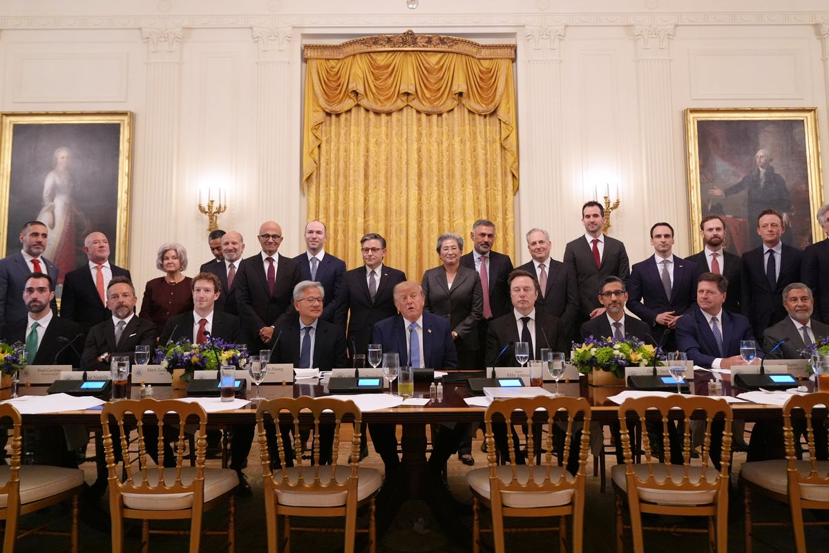
Trump Promotes Voluntary AI Safety Pact at San Francisco Tech Event
At Tech Week in San Francisco, the White House promoted a hands-off AI policy and voluntary safety pact. Industry leaders welcomed the shift toward growth over regulation.

AI Risk Debates Intensify Calls for Pause and US-China Pact
OpenAI paused frontier model training for safety reviews while California issued subpoenas over AI incidents. Officials discussed voluntary standards and potential FTC probes.
The Compass
You just read five takes on one story.
What's your take? Find your political shape in a few minutes.
Take the test